
R e s e a r c h
O p t o e l e c t r o n i c s
M i c r o d i s k s
Within the last decade, semiconductor microdisk resonators have become extremely useful for studying microcavity effects. A microdisk is a thin semiconductor disk surrounded by a lower index material such as air or SiO2. The large index difference between the semiconductor and the surrounding medium allows for strong optical confinement. The circular geometry of the disk permits low loss whispering gallery modes (WGMs) to propagate around the disk periphery through total internal reflection. The geometry of the microdisk is ideal for studying a material system such as GaN in which cleaved facets and several period epitaxial mirror stacks are problematic.
Nonetheless, GaN microdisk development has been hindered by the inability to effectively surround the microdisk with lower index materials. Processing techniques, such as selective wet etching or oxidation, used for optical confinement of GaAs- and InP-based microdisks are not readily available for the GaN system because of its chemical stability. We must use unconventional processing techniques for GaN microdisk fabrication.
One such technique is photoelectrochemical (PEC) etching. PEC etching uses above band gap illumination to generate the excess carriers (specifically holes) needed to etch GaN. Band bending near the material surface causes the holes to be drawn toward the GaN-etchant interface, allowing them to participate in the electrochemical reaction necessary for material removal. Because the etching mechanisms rely heavily on the absorption of incident light, PEC etching is bandgap-selective.
PEC etching has already demonstrated its utility in etching GaN. We have previously reported rapid, bandgap selective lateral etching resulting in the undercut or lift-off of GaN structures. Such etches exhibited finite selectivity and often resulted in rough etch surfaces. In order to fabricate high quality GaN microdisk structures, we must address these issues. In particular, the microdisk structure is extremely sensitive to surface roughness because it can cause scattering losses detrimental to optical performance. Furthermore, to prevent etching into the microdisk itself, we must increase the selectivity of the etch process.
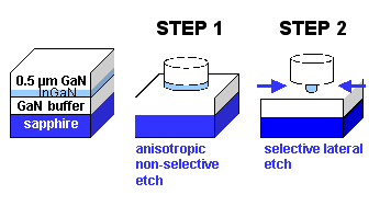
In our work, we use an epitaxial structure grown by MOCVD that includes a 1000 Å In0.12Ga0.88N sacrificial layer. Reactive ion etching is used to define micropillars of various diameters and expose the InGaN sacrificial layer. The GaN microdisks are undercut by using PEC etching to selectively etch the InGaN sacrificial layer. An optical filter is used to filter out light with energy greater than the bandgap of GaN. Thus, etching is prevented in the GaN layers and selective etching of the InGaN sacrificial layer occurs. The PEC etch conditions are optimized for lateral etch rates and smooth undercut surface. Although etch rates as high as 10 µm/min have been obtained, the smoothness of the undercut surface is our most critical parameter in our process. Therefore, our research has been focused on reducing the roughness of the undercut by reducing etchant concentration, varying the spectrum and intensity of the above bandgap light, and experimenting with various epitaxial structures.
|
|||||||
| Process flow for GaN microdisk devices | |||||||
| Design criteria for microdisk lasers | |
||||||
Last updated
The Interdisciplinary Center for Wide Bandgap Semiconductors
The Solid State Lighting and Display Center
Copyright © 2001-2002